. Scientific Frontline: Nanotechnology
Showing posts with label Nanotechnology. Show all posts

Wednesday, November 9, 2022

Novel Nanowire Fabrication Technique Paves Way for Next Generation Spintronics


The challenge of fabricating nanowires directly on silicon substrates for the creation of the next generation of electronics has finally been solved by researchers from Tokyo Tech. Next-generation spintronics will lead to better memory storage mechanisms in computers, making them faster and more efficient.

As our world modernizes faster than ever before, there is an ever-growing need for better and faster electronics and computers. Spintronics is a new system which uses the spin of an electron, in addition to the charge state, to encode data, making the entire system faster and more efficient. Ferromagnetic nanowires with high coercivity (resistance to changes in magnetization) are required to realize the potential of spintronics. Especially L10-ordered (a type of crystal structure) cobalt–platinum (CoPt) nanowires.

Conventional fabrication processes for L10-ordered nanowires involve heat treatment to improve the physical and chemical properties of the material, a process called annealing on the crystal substrate; the transfer of a pattern onto the substrate through lithography; and finally, the chemical removal of layers through a process called etching. Eliminating the etching process by directly fabricating nanowires onto the silicon substrate would lead to a marked improvement in the fabrication of spintronic devices. However, when directly fabricated nanowires are subjected to annealing, they tend to transform into droplets as a result of the internal stresses in the wire.

Monday, October 31, 2022

New catalyst can turn smelly hydrogen sulfide into a cash cow

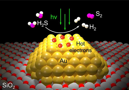
An illustration of the light-powered, one-step remediation process for hydrogen sulfide gas made possible by a gold photocatalyst created at Rice University.
Image Credit: Halas Group/Rice University

Hydrogen sulfide gas has the unmistakable aroma of rotten eggs. It often emanates from sewers, stockyards and landfills, but it is particularly problematic for refineries, petrochemical plants and other industries, which make thousands of tons of the noxious gas each year as a byproduct of processes that remove sulfur from petroleum, natural gas, coal and other products.

In a published study in the American Chemical Society’s high-impact journal ACS Energy Letters, Rice engineer, physicist and chemist Naomi Halas and collaborators describe a method that uses gold nanoparticles to convert hydrogen sulfide into high-demand hydrogen gas and sulfur in a single step. Better yet, the one-step process gets all its energy from light. Study co-authors include Rice’s Peter Nordlander, Princeton University’s Emily Carter and Syzygy Plasmonics’ Hossein Robatjazi.

“Hydrogen sulfide emissions can result in hefty fines for industry, but remediation is also very expensive,” said Halas, a nanophotonics pioneer whose lab has spent years developing commercially viable light-activated nanocatalysts. “The phrase ‘game-changer’ is overused, but in this case, it applies. Implementing plasmonic photocatalysis should be far less expensive than traditional remediation, and it has the added potential of transforming a costly burden into an increasingly valuable commodity.”

Monday, October 24, 2022

Molecular cage protects precious metals in catalytic converters

Stable catalyst illustration
Source/Credit: Slac National Accelerator Laboratory

Sometimes, solutions to environmental problems can have environmentally unfriendly side effects. For example, while most gas-powered cars have a catalytic converter that transforms engine emission pollutants into less harmful gases, this comes with a tradeoff: Catalytic converters contain precious metals such as platinum and palladium.

The good thing about these precious metals is that they act as catalysts that help break down pollutants, with a suite of properties that make them the best elemental candidates for this chemical job. But they are also rare, which makes them expensive, and extracting them from the earth produces its own pollution.

However, in a paper published October 24 in Nature Materials, researchers at the SUNCAT Center for Interface Science and Catalysis and the Precourt Institute for Energy at Stanford University and the Department of Energy’s SLAC National Accelerator Laboratory reported a way of encapsulating catalysts that could reduce the number of precious metals catalytic converters need to work, which could in turn reduce the practice of precious metal mining.

“I think the material we made could knock down the number of precious metals used in a catalytic converter by 50 precent, which would mean a lot once you multiply that by the nearly 1.5 billion cars we now have in circulation on the planet,” said Matteo Cargnello, the new study's senior author and an assistant professor of chemical engineering at Stanford University.

Friday, October 21, 2022

Ural Scientists Created Nanoparticle Growth Technology

The new material is suitable for solar cells, biosensors, and other systems working on quantum principles.
Photo credit: Vladimir Petrov

Physicists at Ural Federal University and their colleagues from the Institute of Electrophysics, Ural Branch of the Russian Academy of Sciences, and the Institute of Ion Plasma and Laser Technologies, Academy of Sciences, have developed a technology for growing nonspherical nanoparticles that are synthesized by ion implantation. With the new technique, it is possible to grow nanoparticles of different shapes and thus obtain the necessary properties and control them. The technology is applicable to different metals, both noble metals such as gold, silver, platinum, and "ordinary", the scientists assure. A description of the technology and the results of the first experiments - copper implantation in ceramics - are presented in the Journal of Physics and Chemistry of Solids.

"By changing the shape of nanoparticles from spherical to non-spherical, we were able to increase the range of optical absorption. This, in turn, is the basis for further converting the absorbed energy into electricity and heat. As a result, we can get more functional sensors and increase their sensitivity range. If such nanoparticles are built into lasers, their power will increase. If we talk about sensors, their sensitivity will increase. As for sensors, their response time will change. This is all due to the peculiarity of plasmon resonance, which leads to the fact that around the nanoparticles there is an amplified electric field," explains study co-author Arseny Kiryakov, Associate Professor at the Department of Physical Techniques and Devices for Quality Control at UrFU.

Wednesday, October 19, 2022

Thinnest ferroelectric material ever paves the way for new energy-efficient devices

A representation of a two-dimensional ferroelectric material.
Image credit: UC Berkeley/Suraj Cheema.

As electronic devices become smaller and smaller, the materials that power them need to become thinner and thinner. Because of this, one of the key challenges scientists face in developing next-generation energy-efficient electronics is discovering materials that can maintain special electronic properties at an ultrathin size.

Advanced materials known as ferroelectrics present a promising solution to help lower the power consumed by the ultrasmall electronic devices found in cell phones and computers. Ferroelectrics — the electrical analog to ferromagnets — are a class of materials in which some of the atoms are arranged off-center, leading to a spontaneous internal electric charge or polarization. This internal polarization can reverse its direction when scientists expose the material to an external voltage. This offers great promise for ultralow-power microelectronics.

Unfortunately, conventional ferroelectric materials lose their internal polarization below around a few nanometers in thickness. This means they are not compatible with current-day silicon technology. This issue has previously prevented the integration of ferroelectrics into microelectronics.

But now a team of researchers from the University of California at Berkeley performing experiments at the U.S.

Tuesday, October 11, 2022

Graphene Boosts Flexible and Wearable Electronics


At 200 times stronger than steel, graphene has been hailed as a super material of the future since its discovery in 2004. The ultrathin carbon material is an incredibly strong electrical and thermal conductor, making it a perfect ingredient to enhance semiconductor chips found in many electrical devices.

But while graphene-based research has been fast-tracked, the nanomaterial has hit roadblocks: in particular, manufacturers have not been able to create large, industrially relevant amounts of the material. New research from the laboratory of Nai-Chang Yeh, the Thomas W. Hogan Professor of Physics, is reinvigorating the graphene craze.

In two new studies, the researchers demonstrate that graphene can greatly improve electrical circuits required for wearable and flexible electronics such as smart health patches, bendable smartphones, helmets, large folding display screens, and more.

In one study, published in ACS Applied Materials & Interfaces, the researchers grew graphene directly onto thin two-dimensional copper lines commonly used in electronics. The results showed that the graphene not only improved the lines' conducting properties but also protected the copper-based structures from usual wear and tear. For instance, they showed that graphene-coated copper structures could be folded 200,000 times without damage, as compared to the original copper structures, which started cracking after 20,000 folds. The results demonstrate that graphene can help create flexible electronics with longer lifetimes.

Wednesday, September 28, 2022

Scientists chip away at a metallic mystery, one atom at a time

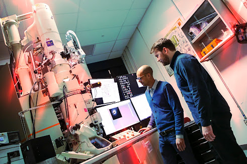
In this photo from 2020, Christopher Barr, right, a former Sandia National Laboratories postdoctoral researcher, and University of California, Irvine, professor Shen Dillon operate the In-situ Ion Irradiation Transmission Electron Microscope. Barr was part of a Sandia team that used the one-of-a-kind microscope to study atomic-scale radiation effects on metal.
Photo credit: Lonnie Anderson

Gray and white flecks skitter erratically on a computer screen. A towering microscope looms over a landscape of electronic and optical equipment. Inside the microscope, high-energy, accelerated ions bombard a flake of platinum thinner than a hair on a mosquito’s back. Meanwhile, a team of scientists studies the seemingly chaotic display, searching for clues to explain how and why materials degrade in extreme environments.

Based at Sandia, these scientists believe the key to preventing large-scale, catastrophic failures in bridges, airplanes and power plants is to look — very closely — at damage as it first appears at the atomic and nanoscale levels.

“As humans, we see the physical space around us, and we imagine that everything is permanent,” Sandia materials scientist Brad Boyce said. “We see the table, the chair, the lamp, the lights, and we imagine it’s always going to be there, and it’s stable. But we also have this human experience that things around us can unexpectedly break. And that’s the evidence that these things aren’t really stable at all. The reality is many of the materials around us are unstable.”

Thursday, September 22, 2022

Heat-resistant nanophotonic material could help turn heat into electricity

His artist’s rendering shows the material reflecting infra-red light while letting other wavelengths pass through.
Image credit: Andrej Lenert

A new nanophotonic material has broken records for high-temperature stability, potentially ushering in more efficient electricity production and opening a variety of new possibilities in the control and conversion of thermal radiation.

Developed by a University of Michigan-led team of chemical and materials science engineers, the material controls the flow of infrared radiation and is stable at temperatures of 2,000 degrees Fahrenheit in air, a nearly twofold improvement over existing approaches.

The material uses a phenomenon called destructive interference to reflect infrared energy while letting shorter wavelengths pass through. This could potentially reduce heat waste in thermophotovoltaic cells, which convert heat into electricity but can’t use infrared energy, by reflecting infrared waves back into the system. The material could also be useful in optical photovoltaics, thermal imaging, environmental barrier coatings, sensing, camouflage from infrared surveillance devices and other applications.

Friday, September 16, 2022

Improved Mineralized Material Can Restore Tooth Enamel

Scientists tested the effectiveness of the new enamel coating on real healthy teeth.
Photo credit: Danil Ilyukhin

Scientists have perfected hydroxyapatite, a material for mineralizing bones and teeth. By adding a complex of amino acids to hydroxyapatite, they were able to form a dental coating that replicates the composition and microstructure of natural enamel. Improved composition of the material repeats the features of the surface of the tooth at the molecular and structural level, and in terms of strength surpasses the natural tissue. The new method of dental restoration can be used to reduce the sensitivity of teeth in case of abrasion of enamel or to restore it after erosion or improper diet. The study and experimental results are published in Results in Engineering.

"Tooth enamel has a protective function, but unfortunately, its integrity can be destroyed by, for example, abrasion, erosion or microfractures. If the surface of the tissue is not repaired in time, the enamel lesion will affect the dentin and then the pulp of the tooth. Therefore, it is necessary to restore the enamel surface to a healthy level or build up additional layers on the surface if it has become very thin. We have created a biomimetic (i.e., mimicking natural) mineralized layer whose nanocrystals replicate the ordering of apatite nanocrystals of tooth enamel. We also found out that the designed layer of hydroxyapatite has increased nanohardness that exceeds that of native enamel," says Pavel Seredin, Leading Specialist of Research and Education Center "Nanomaterials and Nanotechnologies", Ural Federal University, Head of the Department of Solid State Physics and Nanostructures at Voronezh State University.

Friday, September 9, 2022

Scientists Create Mathematical Model for Nanoparticle and Virus Dynamics in Cells

Dmitry Aleksandrov and Sergey Fedotov (left to right) determined the behavior of viruses in cells.
 Photo credit: Ilya Safarov

Physicists and mathematicians at the Ural Federal University and the University of Manchester have for the first time created a complex mathematical model that calculates the distribution of nanoparticles (particularly viruses) in living cells. Using the mathematical model, scientists have figured out how nanoparticles cluster (merge into a single particle) inside cells, namely in cellular endosomes, which are responsible for sorting and transporting proteins and lipids.

These calculations will be useful for medical purposes because, on the one hand, they show how viruses behave when they enter cells and tend to replicate. On the other hand, the model allows the exact amount of medication needed for therapy to be as effective as possible and with minimal side effects. The scientists published the model description and calculation results in Crystals, Cancer Nanotechnology and Mathematics.

"The processes in cells are extremely complex, but in simple terms, viruses use different variants to reproduce. Some deliver genetic material directly into the cytoplasm. Others use the endocytosis pathway: they deliver the viral genome by releasing it from the endosomes. If viruses stay in the endosomes, the acidity increases there, and they die in the lysosomes. So, our model allowed us to find out, first of all, when and which viruses "escape" from endosomes in order to survive. For example, some influenza viruses are low-pH-dependent viruses; they fuse with the endosome membrane and release their genome into the cytoplasm. Secondly, we found out that it is easier for viruses to survive in endosomes during clustering, when two particles merge and tend to form a single particle," says Dmitry Aleksandrov, Head of the Multi-Scale Mathematical Modeling Laboratory at UrFU.

Sunday, September 4, 2022

Researchers devise tunable conducting edge

In their experiments, the researchers stacked monolayer WTe2 with Cr2Ge2Te6, or
CGT. Credit: Shi lab/UC Riverside

A research team led by a physicist at the University of California, Riverside, has demonstrated a new magnetized state in a monolayer of tungsten ditelluride, or WTe2, a new quantum material. Called a magnetized or ferromagnetic quantum spin Hall insulator, this material of one-atom thickness has an insulating interior but a conducting edge, which has important implications for controlling electron flow in nanodevices.

In a typical conductor, electrical current flows evenly everywhere. Insulators, on the other hand, do not readily conduct electricity. Ordinarily, monolayer WTe2 is a special insulator with a conducting edge; magnetizing bestows upon it more unusual properties.

“We stacked monolayer WTe2 with an insulating ferromagnet of several atomic layer thickness — of Cr2Ge2Te6, or simply CGT — and found that the WTe2 had developed ferromagnetism with a conducting edge,” said Jing Shi, a distinguished professor of physics and astronomy at UCR, who led the study. “The edge flow of the electrons is unidirectional and can be made to switch directions with the use of an external magnetic field.”

Shi explained that when only the edge conducts electricity, the size of the interior of the material is inconsequential, allowing electronic devices that use such materials to be made smaller — indeed, nearly as small as the conducting edge. Because devices using this material would consume less power and dissipate less energy, they could be made more energy efficient. Batteries using this technology, for example, would last longer.

Tuesday, August 30, 2022

Researchers produce nanodiamonds capable of delivering medicinal and cosmetic remedies through the skin

Nanodiamond applied on skin samples and penetrated through all skin layers: nanodiamond concentration reduces as the layer is deeper
Credit: Prof. Dror Fixler, Bar-Ilan University 

The skin is one of the largest and most accessible organs in the human body, but penetrating its deep layers for medicinal and cosmetic treatments still eludes science.

Although there are some remedies -- such as nicotine patches to stop smoking -- administered through the skin, this method of treatment is rare since the particles that penetrate must be no larger than 100 nanometers (one thousandth of a centimeter). Creating effective tools using such tiny particles is a great challenge. Because the particles are so small and difficult to see, it is equally challenging to determine their exact location inside the body – information necessary to ensure that they reach the intended target tissue. Today such information is obtained through invasive, often painful, biopsies.

A novel approach, developed by researchers at Bar-Ilan University in Israel, provides an innovative solution to overcoming both of these challenges. Combining techniques in nanotechnology and optics, they produced tiny (nanometric) diamond particles so small that they are capable of penetrating skin to deliver medicinal and cosmetic remedies. In addition, they created a safe, laser-based optical method that quantifies nanodiamond penetration into the various layers of the skin and determines their location and concentration within body tissue in a non-invasive manner – eliminating the need for a biopsy.

Tuesday, August 23, 2022

No Fib: NIST Unmasks a Superfast Process for Nanoscale Machining

NIST researchers have demonstrated that a focused ion beam (FIB) can fabricate microscopic devices with fine resolution and without sacrificing high speed. Left: The conventional FIB process requires a narrow, low-current ion beam to fabricate a miniature version of a lighthouse lens in silica glass with fine resolution. Because the beam has a low current of ions, the method is time consuming. Right: Placing a protective layer of chromium oxide over the silica glass enables machinists to use a much higher-current ion beam, allowing them to fabricate the same lenses 75 times faster. 
Credit: Andrew C. Madison, Samuel M. Stavis/NIST

Cutting intricate patterns as small as several billionths of a meter deep and wide, the focused ion beam (FIB) is an essential tool for deconstructing and imaging tiny industrial parts to ensure they were fabricated correctly. When a beam of ions, typically of the heavy metal gallium, bombards the material to be machined, the ions eject atoms from the surface—a process known as milling—to sculpt the workpiece.

Beyond its traditional uses in the semiconductor industry, the FIB has also become a critical tool for fabricating prototypes of complex three-dimensional devices, ranging from lenses that focus light to conduits that channel fluid. Researchers also use the FIB to dissect biological and material samples to image their internal structure.

Friday, August 12, 2022

Breast cancer cells use forces to open up channels through tissue

An illustrated microscope view of a 3D culture of cancer cells. A cancer cell generates forces (in red) moving the tissue material farther. The new technique detects the material movement to compute cellular forces.
Image Credit: Juho Pokki/Aalto University

Research to understand how cancers grow and spread has conventionally been done on two-dimensional, flat cultures of cells, which is very different to the three-dimensional structure of cells in the body. 3D cell cultures that incorporate tissue material have been developed, but the methods to measure how cancer cells use forces to spread have been lacking.

Now, researchers have developed a new method for 3D culture to accurately quantify how cancer cells generate forces to spread within tissue. ‘We have applied the method for investigation of early progression of breast cancer,’ says Juho Pokki, a principal investigator at Aalto University who led the research.

This study, a collaboration between scientists at Aalto University and Stanford University, was published in the journal Nano Letters.

Sunday, August 7, 2022

University Scientists Work on Advanced Nanomaterials

Under the leadership of Vladimir Shur, several scientific groups are conducting research.
Credit: Ilya Safarov

Synthesis of new materials with unique characteristics for practical applications is the goal of the project "Experimental and Theoretical Investigation of Physical Properties of Advanced Nanomaterials," which was launched at Ural Federal University. The state program for supporting universities, Priority 2030, in which the Ural Federal University is a participant, is also focused on this very goal. The project will last until 2025 inclusive.

The project is implemented by six groups consisting of 40 scientists. Researchers are united by general objectives: to study and describe the formation processes and physical features of micro- and nanoscale structures to create promising solid-state materials based on segmentelectrics, dielectrics, semiconductors, and superconductors.

The project is led by the world-renowned scientist Vladimir Shur, Professor at the Department of Condensed Matter Physics and Nanoscale Systems, Chief Researcher at the Section of Optoelectronics and Semiconductor Technology, and Head of the Ural Multiple Access Center "Modern Nanotechnologies". One of the experimental-theoretical groups under his leadership studies the evolution of domain structures in ferroelectric crystals.

"Segnetoelectrics have a domain structure that can be changed by applying an external electric field. The creation of stable domain structures with a given geometry is a rapidly developing field of science and technology - domain engineering. Targeted design of micro- and nanoscale domain structures makes it possible to significantly improve a variety of important application-specific characteristics of segmentelectrics," says Vladimir Shur.

Wednesday, July 27, 2022

Scientists use copper nanowires to combat the spread of diseases

Left: Scanning electron microscopy image of the CuNW network on a copper-sprayed surface. Right: Up-close image of CuNW nanowire, which is about 60 nm in diameter, approximately 100x smaller than a human hair.
Resized Image using AI by SFLORG
Credit: Ames National Laboratory

An ancient metal used for its microbial properties is the basis for a materials-based solution to disinfection. A team of scientists from Ames National Laboratory, Iowa State University, and University at Buffalo developed an antimicrobial spray that deposits a layer of copper nanowires onto high-touch surfaces in public spaces. The spray contains copper nanowires (CuNWs) or copper-zinc nanowires (CuZnNWs) and can form an antimicrobial coating on a variety of surfaces. This research was initiated by the COVID-19 pandemic, but the findings have wider-reaching applications.

People have taken advantage of copper’s antimicrobial properties since 2400 B.C. to treat and prevent infections and diseases. It has been proven effective for inactivating viruses, bacteria, fungi, and yeasts when they are directly in contact with the metal. According to Jun Cui, a scientist at Ames Lab and one of the lead researchers on the project, “copper ion can penetrate the membrane of a virus and then insert itself into the RNA chain, and completely disable the virus from duplicating itself.”

Amidst the pandemic, “The DOE asked researchers, what can you do to help to mitigate this COVID situation?” Cui said. Ames Lab is known for work in materials science, not a field that often intersects with disease research. However, Cui’s team came up with the idea to apply copper’s antimicrobial properties to help reduce the spread of COVID.

Cui explained their idea came from a separate project they were working on, which is a copper ink designed for printing copper nanowires used in flexible electronic devices. “So, the thinking is, this is ink, and I can dilute it with water or even ethanol, and then just spray it. Whatever the surface, I spray it once and coat it with a very light layer of copper nanowire,” he said.

Monday, June 27, 2022

New optical device could help solar arrays focus light, even under clouds

Different stages of the graded index glass pyramid fabrication: when in optical contact with a solar cell, the pyramid at the final step (bottom right corner) absorbs and concentrates most of the incident light and appears dark.
Image credit: Nina Vaidya

Stanford engineers’ optical concentrator could help solar arrays capture more light even on a cloudy day without tracking the sun

Researchers imagined, designed, and tested an elegant lens device that can efficiently gather light from all angles and concentrate it at a fixed output position. These graded index optics also have applications in areas such as light management in solid-state lighting, laser couplers, and display technology to improve coupling and resolution.

Even with the impressive and continuous advances in solar technologies, the question remains: How can we efficiently collect energy from sunlight coming from varying angles from sunrise to sunset?

Solar panels work best when sunlight hits them directly. To capture as much energy as possible, many solar arrays actively rotate towards the sun as it moves across the sky. This makes them more efficient, but also more expensive and complicated to build and maintain than a stationary system.

Thursday, June 23, 2022

Boron nitride nanotube fibers get real

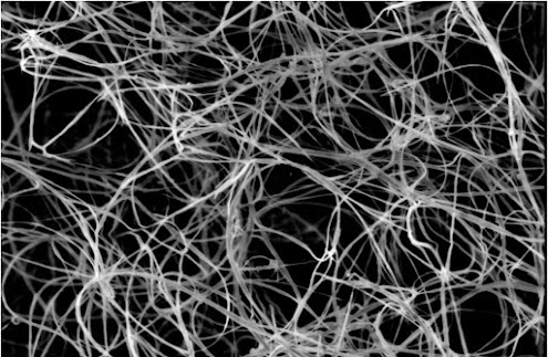
A tangle of unprocessed boron nitride nanotubes seen through a scanning electron microscope. Rice University scientists introduced a method to combine them into fibers using the custom wet-spinning process they developed to make carbon nanotube fibers.
Credit: Pasquali Research Group/Rice University

Boron nitride nanotubes used to be hard to process, according to Rice University researchers. Not anymore.

A Rice team led by professors Matteo Pasquali and Angel Martí has simplified handling of the highly valuable nanotubes to make them more suitable for large-scale applications, including aerospace, electronics and energy-efficient materials.

The researchers reported in Nature Communications that boron nitride nanotubes, aka BNNTs, assemble themselves into liquid crystals under the right conditions, primarily concentrations above 170 parts per million by weight in chlorosulfonic acid.

These liquid crystals consist of aligned BNNTs that are far easier to process than the tangled nanotubes that usually form in solution. The lab proceeded to form fibers and films from the liquid crystalline solutions.

Wednesday, June 22, 2022

Technique Allows Researchers to Align Gold Nanorods with Magnetic Fields

Electron micrograph of gold nanorods overcoated with iron oxide nanoparticles and aligned in a magnetic field.
Image Credit: Mehedi H. Rizvi

An international team of researchers has demonstrated a technique that allows them to align gold nanorods using magnetic fields, while preserving the underlying optical properties of the gold nanorods.

“Gold nanorods are of interest because they can absorb and scatter specific wavelengths of light, making them attractive for use in applications such as biomedical imaging, sensors, and other technologies,” says Joe Tracy, corresponding author of a paper on the work and a professor of materials science and engineering at North Carolina State University.

It is possible to tune the wavelengths of light absorbed and scattered by engineering the dimensions of the gold nanorods. Magnetically controlling their orientation makes it possible to further control and modulate which wavelengths the nanorods respond to.

“In other words, if you can control the alignment of gold nanorods, you have greater control over their optical properties,” Tracy says. “And using magnetic fields to control that alignment means that you can control the alignment without actually touching the nanorods.”

In their technique, the researchers synthesize separate solutions of gold nanorods and iron oxide nanoparticles. Mixing the solutions drives assembly of the iron oxide nanoparticles onto the surface of the gold nanorods. The resulting “coated” nanorods can then be controlled using a low-strength magnetic field.

On the Road to Tiny Transistors, How Flat is Flat?

The general architecture of a traditional MOSFET vs. a 2D FET. A FET (field-effect transistor) is a device for regulating the flow of charge carriers (such as electrons) across a channel with three terminals: a source, a drain, and a gate. A MOSFET (metal oxide semiconductor field effect transistor) is by far the most widely used type of FET and is a building block of modern electronics, used in commercial electronic devices for more than 50 years. One main difference between the traditional 3D MOSFET and the “emerging technology” of the 2D FET is that the channel in a traditional MOSFET is in a 3D material, while a 2D FET’s channel is a 2D material.
Credit: Sean Kelley/NIST

Transistors are the building blocks of modern electronics, used in everything from televisions to laptops. As transistors have gotten smaller and more compact, so have electronics, which is why your cell phone is a super powerful computer that fits in the palm of your hand.

But there’s a scaling problem: Transistors are now so small that they are difficult to turn off. A key device element is the channel that charge carriers (such as electrons) travel across between electrodes. If that channel gets too short, quantum effects allow electrons to effectively jump from one side to another even when they shouldn’t.

One way to get past this sizing roadblock is to use layers of 2D materials – which are only a single atom thick – as the channel. Atomically thin channels can help enable even smaller transistors by making it harder for the electrons to jump between electrodes. One well-known example of a 2D material is graphene, whose discoverers won the Nobel Prize in Physics in 2010. But there are other 2D materials, and many believe they are the future of transistors, with the promise of scaling channel thickness down from its current 3D limit of a few nanometers (nm, billionths of a meter) to less than a single nanometer thickness.

Though research has exploded in this area, one issue has been persistently overlooked, according to a team of scientists from the National Institute of Standards and Technology (NIST), Purdue University, Duke University, and North Carolina State University. The 2D materials and their interfaces – which researchers intend to be flat when stacked on top of each other – may not, in fact, be flat. This non-flatness in turn can significantly affect device performance, sometimes in good ways and sometimes in bad.

Featured Article

Autism and ADHD are linked to disturbed gut flora very early in life

The researchers have found links between the gut flora in babies first year of life and future diagnoses. Photo Credit:  Cheryl Holt Disturb...

Top Viewed Articles