Magnets are used in so many of our everyday objects including cell phones and in the strip of a credit card or a hotel key. They even power the engine in your vacuum.
And as most computers use magnets to store information, finding ever thinner magnets is key to faster, lighter electronics. Graphene, a material that is one atom thick, was discovered in 2004 and won the 2010 Nobel Prize in physics. While graphene is not magnetic itself, it triggered the interest of searching for atomically thin magnets.
In 2017, scientists found an ultrathin, magnetic material just three atoms, or one atomic unit, thick. But this material, called chromium triiodide, had a simple magnetic moment arrangement—the spin of the electrons within the material all aligned in the same direction, either up or down—which means it’s not able to store large amounts of information.
Now, University of Michigan physicist Liuyan Zhao and her team have developed a way to create a more complex magnetic moment arrangement in chromium triiodide, allowing this atomically thin material to store more information and to perhaps process information faster. Their results are published in Nature Physics.
“Over time, people began looking for smaller sizes and more complex forms of magnets in order to make our computers and electronics smaller, thinner and faster. To do this, the material that stores data or does information processing needs to also get smaller and smaller, while their magnetic forms should be more and more exotic,” Zhao said. “In very big, bulky materials, people find all kinds of magnetic forms called spin textures. So in this ultrathin material, we asked: Can we also create those kinds of complex spin textures so that we can store more information?”
To do this, Zhao and her team created an artificial sample by tearing a micron-sized (one millionth of a meter) flake of chromium triiodide into two. The flake of chromium triiodide is bilayer, which means the material is two atomic units, or six atoms, thick. Then, they layered one piece on top of the other and rotated it a tiny amount. Each flake is composed of a crystalline lattice structure, and when one structure is laid over another and rotated a small amount, the crystalline structures interfere with each other and form a periodic structure with a longer wavelength. This also creates an angular mismatch between the two flakes and leads to a superlattice with a longer period called a moiré superlattice.
Think of a wave of water. The ripple of one wave equals one period. But within this wave, water doesn’t actually move forward. Instead, the molecules of water rise and fall in one location. When more energy is added to the wave, the wave crests higher.
Similarly, when the crystalline structures are layered on top of each other, their wave period is doubled. Then, because of the small rotation between the two layers, the atoms in the top layer of the material are slightly offset from the atoms in the lower layer of material near the center of rotation. This further causes a cascading effect of offset atoms throughout the doubled layer of material, which repeats throughout the entire piece of stacked layers at the moiré wavelength.
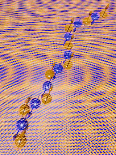
This results in two extremes of offsets within the structure, Zhao says. When the chromium atoms in one layer are arranged right in the center of chromium atoms of the other, their spins like to be in the same direction. When they are off by a third of the distance between the nearest neighboring chromium atoms, their spins favor in the opposite direction. Then between these two areas, their spins become frustrated, not knowing which of the two ways to follow, and could develop new arrangements. They then, for example, can become spiraled. The different kinds of spin orientations within the same material creates more opportunities to store information.
To work with such impossibly thin and delicate materials, the group uses a set of automated micromanipulators under an optical microscope that is hosted in a box filled with ultra high purity nitrogen, which is inert and does not interact with the material the researchers study. The researchers use a common household staple— tape—to peel a 2D layer of material and stamp it onto a substrate of silicon dioxide, a technique developed by the 2010 physics Nobel winners. Using the optical microscope to watch the procedure, the researchers control a set of mechanical arms to lift one layer of the material, twist it slightly, and lay it back down on top of the other layer of material.
“The importance of our work is to demonstrate in these very thin magnets we can design the spin texture by doing this kind of twisting to introduce the moiré superlattices. Different spin arrangements can give quite different physical properties of the magnetic materials we study,” Zhao said. “As compared to many 3D bulky materials, the atomic arrangements are determined by chemistry during growth: you cannot change or manipulate that much. But here, by changing this twist angle between two layers to change the relative distance between atoms, we have the freedom to design and control magnetic properties in 2D moiré superlattices.”
The collaborative work involves scientists from multiple research institutions. Co-authors include Hongchao Xie, Xiangpeng Luo and Kai Sun in the U-M Department of Physics; Gaihua Ye, Zhipeng Ye, Rui He and Haiwen Ge at Texas Tech University; Suk Hyun Sung and Robert Hovden in the U-M Department of Materials Science and Engineering; Emily Rennich in the U-M Department of Mechanical Engineering; and Shaohua Yan, Yang Fu, Shangjie Tian and Hechang Lei at the Renmin University of China.
Source/Credit: University of Michigan
phy120221_01


.jpg)